Friday, May 27, 2011

Mobile Charger using Bike Battery

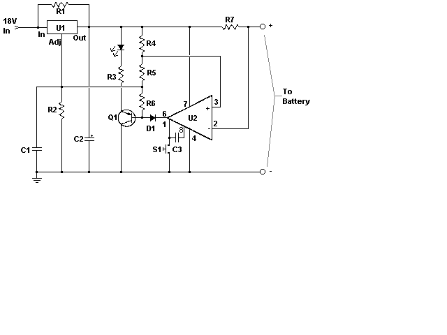
When a surge voltage exceeding maximum voltage rating of the regulator is applied to the input or when a voltage in excess of the input voltage is applied to the output, the regulator will be destroyed. If the input terminal shorts with the ground, the output voltage increases above the input voltage(ground potential)and the charge in the capacitor connected to the output flows into the input side which is also fatal to the regulator. Both these situations can be avoided by using the Zener at the input and the diode D1 across the regulator. Capacitor C1 and C2 provide stability to the regulator and these should be soldered close to the legs of the regulator. Capacitor C3 act as a buffer to give constant voltage in the output.
7805 IC can tolerate maximum 35 volts and its current rating is 1 Amps maximum. Resistor R1 restricts the charging current to around 330 mA as per the Ohms law. Even if the current is low, charging process will not be affected. Slow charging with 80 to 100 mA current is generally advised. But in case of an emergency, quick charging can be done with high current
Assemble the circuit on a Perf board and enclose in a small case that can be fitted near the Bike battery. Use suitable pins to connect with the Mobile phone. Charging current can be tapped from the battery using Alligator Clips. Before using the circuit, double check the connections especially the polarity of connectors and measure output voltage and current using a Digital Multi Meter. The same circuit can be used for charging Mobile battery from 12 volt Car battery or from a 12 volt Solar panel.

Solar Charger

The circuit uses a 12 volt solar panel and a variable voltage regulator IC LM 317. The solar panel consists of solar cells each rated at 1.2 volts. 12 volt DC is available from the panel to charge the battery. Charging current passes through D1 to the voltage regulator IC LM 317. By adjusting its Adjust pin, output voltage and current can be regulated.
VR is placed between the adjust pin and ground to provide an output voltage of 9 volts to the battery. Resistor R3 Restrict the charging current and diode D2 prevents discharge of current from the battery. Transistor T1 and Zener diode ZD act as a cut off switch when the battery is full. Normally T1 is off and battery gets charging current.
When the terminal voltage of the battery rises above 6.8 volts, Zener conducts and provides base current to T1. It then turns on grounding the output of LM 317 to stop charging.

Thursday, May 26, 2011

Car Battery Charger

This charger will quickly and easily charge most any lead acid battery. The charger delivers full current until the current drawn by the battery falls to 150 mA. At this time, a lower voltage is applied to finish off and keep from over charging. When the battery is fully charged, the circuit switches off and lights a LED, telling you that the cycle has finished.

PARTS:-


R1    1    500 Ohm 1/4 W Resistor   
R2    1    3K 1/4 W Resistor   
R3    1    1K 1/4 W Resistor   
R4    1    15 Ohm 1/4 W Resistor   
R5    1    230 Ohm 1/4 W Resistor   
R6    1    15K 1/4 W Resistor   
R7    1    0.2 Ohm 10 W Resistor   
C1    1    0.1uF 25V Ceramic Capacitor   
C2    1    1uF 25V Electrolytic Capacitor   
C3    1    1000pF 25V Ceramic Capacitor   
D1    1    1N457 Diode   
Q1    1    2N2905 PNP Transistor   
U1    1    LM350 Regulator   
U2    1    LM301A Op Amp   
S1    1    Normally Open Push Button Switch   
MISC    1    Wire, Board, Heatsink For U1, Case, Binding Posts or Alligator Clips For Output   

Electronic Stethoscope

Stethoscopes are not only useful for doctors, but home mechanics, exterminators, spying and any number of other uses. Standard stethoscopes provide no amplification which limits their use. This circuit uses op-amps to greatly amplify a standard stethoscope, and includes a low pass filter to remove background noise.


PARTS:-


R1    1    10K 1/4W Resistor  
R2    1    2.2K 1/4W Resistor  
R4    1    47K 1/4W Resistor  
R5, R6, R7    3    33K 1/4W Resistor  
R8    1    56K 1/4W Resistor  
R10    1    4.7K 1/4W Resistor  
R11    1    2.2K to 10K Audio Taper Pot  
R12    1    330K 1/4W Resistor  
R13, R15, R16    3    1K 1/4W Resistor  
R14    1    3.9 Ohm 1/4W Resistor  
C1, C8    2    470uF 16V Electrolytic Capacitor  
C2    1    4.7uF 16V Electrolytic Capacitor  
C3, C4    2    0.047uF 50V Metalized Plastic Film Capacitor  
C5    1    0.1uF 50V Ceramic Disc Capacitor  
C6, C7    2    1000uF 16V Electrolytic Capacitor  
U1    1    TL072 Low Noise Dual Op-Amp  
U4    1    741 Op-Amp  
U5    1    LM386 Audio Power Amp  
MIC    1    Two Wire Electret Microphone  
J1    1    1/8" Stereo Headphone Jack  
Batt1, Batt2    2    9V Alkaline Battery  
LED    1    Red/Green Dual Colour Two Wire LED  
SW    1    DPST Switch  
MISC    1    Stethoscope head or jar lid, rubber sleeve for microphone, board, wire, battery clips, knob for R11    

12V Halogen Lamp Electronics Transformer Circuit Diagram

A halogen lamp is a source of electric light that works by heat-driven light emissions produce from the combination of the halogen gas and the tungsten filament. Below schematic shows the 12V Halogen Lamp Electronics Diagram.
The following file is an application note from ST.com containing description of the 12V Halogen Lamp Electronics Diagram. These lamps are available with voltage ratings of 6, 12 or 24 Volts, and so a transformer is needed in order to provide the lamp with a low voltage supply from either 110V a.c. or 220V a.c. mains. The topology of the circuit is the classic half-bridge. The line voltage is rectified by the full-bridge rectifier, generating a semi-sinusoidal voltage at double the line frequency.
Get more information regarding the 12V Halogen Lamp Electronics Diagram design here.

Monday, May 23, 2011

Electronics Cricket Match Game

Add caption

This electronic cricket is a present for Kids. This simple battery powered circuit can be used to play Cricket Match with your friends. Each LED in the circuit indicates various status of the cricket match like Sixer, Run out, Catch etc.
The Circuit uses two ICs ,one in the Astable mode and the second in the display driver mode. IC1 is wired as an Astable Multivibrator with the timing elements R1, R2 and C1. With the shown values of these components very fast output pulses are generated from the Astable. Output from IC1 passes into the input of IC2 which is the popular Johnson Decade counter CD4017. It has 10 outputs. Of these 8 outputs are used. Output 9 ( pin9) is tied to the reset pin 15 to repeat the cycle. When the input pin 14 of IC2 gets low to high pluses, its output turns high one by one. Resistor R3 keeps the input of IC2 low in stand by state to avoid false When the Push Switch S1 is pressed momentarily, the Astable operates and all the LEDs run very fast sequentially. When S1 is released, any one of the LED stands lit which indicates the status of the match. For example, if LED D7 remains lit, it indicates Sixer and if LED 8 remains lit, it indicates Catch out.
Label each LED for its status as shown in the diagram. Pressing of S1 simulates Bowling and Running LEDs indicates running of Batsman.

Electronics Dog Repellent


The electronic dog repellent circuit diagram below is a high output ultrasonic transmitter which is primarily intended to act as a dog and cat repeller, which can be used individuals to act as a deterrent against some animals. It should NOT be relied upon as a defence against aggressive dogs but it may help distract them or encourage them to go away and do not consider this as an electronic pest repeller.

The ultrasonic dog repellant uses a standard 555 timer IC1 set up as an oscillator using a single RC network to give a 40 kHz square wave with equal mark/space ratio. This frequency is above the hearing threshold for humans but is known to be irritating frequency for dog and cats.
Since the maximum current that a 555 timer can supply is 200mA an amplifier stage was required so a high-power H-bridge network was devised, formed by 4 transistors TR1 to TR4. A second timer IC2 forms a buffer amplifier that feeds one input of the H-bridge driver, with an inverted waveform to that of IC1 output being fed to the opposite input of the H-bridge.
For more electronic dog repeller circuits check the related links bellow.
This means that conduction occurs through the complementary pairs of TR1/TR4 and TR2/TR3 on alternate marks and spaces, effectively doubling the voltage across the ultrasonic transducer, LS1. This is optimised to generate a high output at ultrasonic frequencies.
This configuration was tested by decreasing the frequency of the oscillator to an audible level and replacing the ultrasonic transducer with a loudspeaker; the results were astounding. If the dog repellent circuit was fed by a bench power supply rather than a battery that restrict the available current, the output reached 110dB with 4A running through the speaker which is plenty loud enough!
The Dog and Cat repellant was activated using a normal open switch S1 to control the current consumption, but many forms of automatic switching could be used such as pressure sensitive mats, light beams or PIR sensors. Thus it could be utilise as part of a dog or cat deterrent system to help prevent unwanted damage to gardens or flowerbeds, or a battery powered version can be carried for portable use. Consider also using a lead-acid battery if desired, and a single chip version could be built using the 556 dual timer IC to save space and improve battery life.

Sunday, May 22, 2011

Automatic Fan Controller

Th1, the 50K thermistor, is a standard type. Mine was a bar or rectangular looking thingy. Available from Tandy/Radio-Shack. Almost any type will do. I experimented with different models from 22K to 100K
and all worked fine after replacing the trimmer pot. The one used in the above circuit diagram was a 50K model. This 50K was measured at exactly 25 °C and with 10% tolerance. The resistance increases as the surrounding temperature decreases. Tolerance for my application (cooling a large powersupply coolrib) is 10%. Another name for this thing is 'NTC'. NTC stands for "Negative Temperature Coefficient" which means when the surrounding temperature decreases the resistance of this thermistor will increase. I replaced my thermistor for a 60K hermetically
sealed glass type since the environment for my application may contain corrosive particles which may affect performance on a future date. P1 is a regular Bourns trimmer and adjusts a wide range of temperatures for this circuit.

I used the 10-turn type for a bit finer adjustment but the regular type will work for your application.
R1 is a 'security' resistor just in case the trimmer pot P1 is adjusted all the way to '0' ohms. At which time the thermistor would get the full 12 volt and it will get so hot that it puts blisters on your fingers... :-)R3 feeds a bit of hysteresis back into the op-amp to eliminate relay 'chatter' when the temperature of the thermistor reaches its threshold point. Depending on your application and the type you use for Q1 and Re1, start with 330K or so and adjust its value downwards until your satisfied. The value of 150K shown in the diagram worked for me. Decreasing the value of R2 means more hysteresis, just don't use more then necessary. Or temporarily use a trimmer pot and read off the value. 120K worked for me.

Transistor Q1 can be a 2N2222(A), 2N3904, NTE123A, ECG123A, etc. Not critical at all. It acts only as a switch for the relay so almost any type will work, as long as it can provide the current needed to activate the relay's coil. D1, the 1N4148, acts as a spark arrestor when the contacts of the relay open and eliminates false triggering. For my application the 1N4148 was good enough since the tiny relay I used was only 1 amp.

However, you can use a large variety of diodes here, my next choice would be a regular purpose 1N4001 or something and should be used if your relay type can handle more then 1 amp. If you like to make your own pcb, try the one above. The pcb is fitted with holes for the relay but may not fit your particular relay. It was designed for a Aromat HB1-DC12V type.

The variety and model of relays is just to great. How to mount it then? Well, I left ample space on the pcb to mount your relay. You can even mount it up-side-down and connect the wires individually. Use Silicon glue, cyanoacrylate ester (crazy glue), or double-sided tape to hold the relay in place. Works well. Note that the pcb and layout is not according to the circuit diagram in regards to the hookup of the fans. The PCB measures approximately 1.5 x 3 inches (4.8 x 7.6mm) If you print the pcb to an inkjet printer it is probably not to scale. Try to fit a 8-pin ic socket on the printed copy to make sure it fits before making the pcb...

Saturday, May 21, 2011

Simple Digital Security System

You can use this simple and reliable
security system as a watchdog
by installing the sensing
loops around your building. You have
to stretch the loop wires two feet above
the ground to sense the unauthorised
entry into your premises.
Wire loops 1, 2 and 4 are connected
to the A, B and C inputs of 7-segment
decoder 4511 (IC1), respectively, while
the D input of IC1 is grounded permanently.
The loops are also connected to
a dual 3-input NOR gate and inverter
CD4000 (IC2) to activate the alarm.
Fig. 1 shows the circuit of the digital
security system, while Fig. 2 shows
the proposed wiring diagram for the
loops around the premises. Before using
this security system, make sure
that loops shown in Fig. 2 are con-
�� PHERDAUS ISLAM nected as shown in Fig. 1. If you don’t
want to use a buzzer, switch it off by
opening switch S2.
The circuit works off a 9V regulated
power supply. However, battery
back-up is recommended. A commoncathode,
7-segment display (LTS543)
is used for displaying whether the
loops are intact or not.
If loop 1 is broken, the display will
show ‘1’. If two or all the three loops
are broken, the display will show the
sum of the respective broken loop

Smoke Alarm Using 555

The smoke alarm circuit presented here is based on the readily available photon-coupled interrupter module and timer IC NE555. The photo interrupter module is used as the smoke detector, while timer 555 is wired in astable configuration as an AF oscillator for sounding alarm via a loudspeaker.

Circuit diagram of  Smoke Alarm Using 555: Click on image to enlarge


In the absence of any smoke, the gap of photo interrupter module is clear and the light from LED falls on the phototransistor through the slot. As a result, the collector of phototransistor is pulled towards ground. This causes reset pin 4 of IC 555 to go low. Accordingly, the timer is reset and hence the alarm does not sound.

However, when smoke is present in the gap of the photo interrupter module, the light beam from LED to the phototransistor is obstructed. As a result, the phototransistor stops conducting and pin 4 (reset) of IC 555 goes high to activate the alarm.

Note: The unit must be housed inside an enclosure with holes to allow entry of smoke.

Simple electronics Code Lock System

SIMPLE ELECTRONIC
CODE LOCK
The circuit diagram of a simple electronic
code lock is shown in figure.
A 9-digit code number is used
to operate the code lock.
When power supply to the circuit is
turned on, a positive pulse is applied to
the RESET pin (pin 15) through capacitor
C1. Thus, the first output terminal
Q1 (pin 3) of the decade counter IC (CD
4017) will be high and all other outputs
(Q2 to Q10) will be low. To shift the high
state from Q1 to Q2, a positive pulse must
be applied at the clock input terminal (pin
14) of IC1. This is possible only by pressing
the push-to-on switch S1 momentarily.
On pressing switch S1, the high state
shifts from Q1 to Q2.
Now, to change the high state from
Q2 to Q3, apply another positive pulse at
pin 14, which is possible only by pressing
switch S2. Similarly, the high state can
be shifted up to the tenth output (Q10)
by pressing the switches S1 through S9
sequentially in that order. When Q10 (pin
11) is high, transistor T1 conducts and
energises relay RL1. The relay can be
used to switch ‘on’ power to any electrical
appliance.
Diodes D1 through D9 are provided
to prevent damage/malfunctioning of the
IC when two switches corresponding to
‘high’ and ‘low’ output terminals are
pressed simultaneously. Capacitor C2 and
resistor R3 are provided to prevent noise
during switching action.
Switch S10 is used to reset the
circuit manually. Switches S1 to S10
can be mounted on a keyboard panel,
and any number or letter can be used to
mark them. Switch S10 is also placed
together with other switches so that any
stranger trying to operate the lock frequently
presses the switch S10, thereby
resetting the circuit many times. Thus,
he is never able to turn the relay ‘on’. If
necessary, two or three switches can
be connected in parallel with S10 and
placed on the keyboard panel for more
safety.
A 12V power supply is used for the
circuit. The circuit is very simple and can
be easily assembled on a general-purpose
PCB. The code number can be easily
changed by changing the connections to
switches (S1 to S9).

Electronics Jam

This jam circuit can be used in
quiz contests wherein any participant
who presses his button
(switch) before the other contestants,
gets the first chance to answer a question.
The circuit given here permits up
to eight contestants with each one allotted
a distinct number (1 to 8). The
display will show the number of the contestant
pressing his button before the
others. Simultaneously, a buzzer will
also sound. Both, the display as well as
the buzzer have to be reset manually
using a common reset switch.
Initially, when reset switch S9 is momentarily
pressed and released, all outputs
of 74LS373 (IC1) transparent latch
go ‘high’ since all the input data lines
are returned to Vcc via resistors R1
through R8. All eight outputs of IC1
are connected to inputs of priority encoder
74LS147 (IC2) as well as 8-input
NAND gate 74LS30 (IC3). The output
of IC3 thus becomes logic 0 which, after
inversion by NAND gate N2, is applied
to latch-enable pin 11 of IC1. With all
input pins of IC2 being logic 1, its BCD
output is 0000, which is applied to 7-
segment decoder/driver 74LS47 (IC6) after
inversion by hex inverter gates inside
74LS04 (IC5). Thus, on reset the
display shows 0.
When any one of the push-to-on
switches—S1 through S8—is pressed,
the corresponding output line of IC1 is
latched at logic 0 level and the display
indicates the number associated with
the specific switch. At the same time,
Electronic Jam
RAJESH K.P.
output pin 8 of IC3 becomes high, which
causes outputs of both gates N1 and
N2 to go to logic 0 state. Logic 0 output
of gate N2 inhibits IC1, and thus pressing
of any other switch S1 through S8
has no effect. Thus, the contestant who
presses his switch first, jams the display
to show only his number. In the
unlikely event of simultaneous pressing
(within few nano-seconds difference)
of more than one switch, the higher
priority number (switch no.) will be
displayed. Simultaneously, the logic 0
output of gate N1 drives the buzzer via
pnp transistor BC158 (T1). The buzzer
as well the display can be reset (to
show 0) by momentary pressing of reset
switch S9 so that next round may
start.
Lab Note: The original circuit sent
by the author has been modified as it
did not jam the display, and a higher
number switch (higher priority), even
when pressed later, was able to change
the displayed number.